Manufacturability in Flex Circuits Designs
The use of flexible printed circuit boards (PCBs), either stand-alone or to connect rigid areas in the same panel, is increasing rapidly. These devices are often used in the same applications as rigid PCBs but provide significant advantages such as space savings, weight reduction and assembly time reduction. While these devices are not as robust as rigid PCBs they can perform the same electrical functions and are ideal for replacing wire harnesses, which can be bulky and difficult to assemble.
While flex circuits are less tolerant to manufacturability issues than rigid PCBs, there are a number of design-for-manufacture (DFM) techniques that can help ensure a successful flex circuits project. These methods are not only cost-effective, but they can also reduce production times and prevent assembly errors.
For example, it is important to determine up front whether the flex circuits sections will be required to flex repeatedly during product operation (dynamic flexing application) or if they will remain static (static flexing application). This will determine how much copper thickness and what type of insulator material is required. If the flex section is required to be dynamic, it should have a larger bend radius than one for a static application because this will allow it to tolerate multiple bending events over its lifetime.
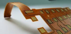
How to Ensure Manufacturability in Flex Circuits Designs
Another key consideration is the hole-to-bend distance. If a hole is close to a bend area, it must be positioned further away from that region in order to avoid damage to the component during the manufacturing process. The designer should also consider how to route the traces near the bend areas. Ideally, traces should be staggered and not run adjacent to each other on adjacent layers. This will distribute the stress more evenly, preventing potential copper failure at the bend location.
Lastly, the pad size and shape should be carefully considered for a successful flex circuits design. Using too large a pad can result in excessive stresses and shorting between the pads, while too small a pad may not provide adequate contact surface for soldering. A good rule of thumb is to choose a pad size that is equal to or slightly larger than the thickness of the copper trace.
The fundamental structure of a flex circuit involves a flexible substrate material, typically polyimide, known for its excellent thermal stability and flexibility. Copper traces are etched or printed on this substrate to create the circuit pathways. Protective layers, such as coverlays or overlays, shield these conductive paths from environmental hazards like dust, moisture, and mechanical wear. The flexibility of the substrate and the durability of the protective layers make these circuits reliable even under demanding conditions.
There are many other issues that must be addressed to ensure a successful flex circuits design, but by following these Dos and Don’ts you can minimize the risks of a failed design. Keeping these guidelines in mind will not only increase your chances of success, but it will also significantly reduce assembly time and costs by eliminating human errors. And most importantly, it will guarantee that your flex circuits will function correctly and reliably for the life of the device. This will ultimately increase the end user’s confidence in your product.
)