
Flex Circuit PCB
A flex circuit is a PCB designed to be flexible and able to bend or conform to the form factor of a product. Flex or rigid-flex PCBs are used when the design calls for complex electronic components to be able to be connected in a 3D manner, such as in a mobile device that needs to be able to fold or bend in its normal operation (dynamic application). They are also useful in applications where space constraints and production costs necessitate a more rigid form factor, but the application requires electrical connections that are not possible with traditional hand wiring or rigid board assemblies.
Rigid flex circuits are usually multilayer and have rigid sections that are interconnected with flexible ones to offer the best of both worlds in terms of flexibility and structural integrity. The rigid sections are often built up from common rigid flex PCB laminates such as FR-4 and similar materials. The conductive copper layer of the flexible section is typically adhered to the substrate using an adhesive or vapour deposition. A flex circuit ribbon is then sandwiched between the rigid sections of the board and conductors routed through it.
When designing a flex or rigid-flex circuit, it is important to keep in mind that the conductive paths of copper must be offset from one another in order to avoid stress concentration in the outermost areas of the ribbon during bending and flexing. This is done to prevent the outermost edges of the conductors from forming sharp corners, which could damage the PCB and reduce its lifespan.
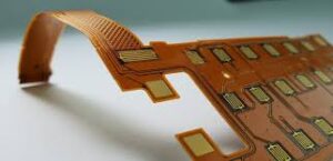
What Is a Flex Circuit PCB?
After the conductive layers are in place, the PCB must undergo an etching and a copper plating process in order to make it functional and ready for assembly. A coverlay is then applied to the surface of the circuit to protect it from contamination in the subsequent drilling, soldering and inserting processes. A stiffener is also added to support the flex circuit during these processes.
Conductors on a flex circuit are typically etched using a metal foil that is available in various thicknesses. The most common and economical choice is copper because it offers a good balance of cost, physical properties and performance attributes. However, other metals like gold and silver are sometimes used in high-performance applications where the traces must be extremely thin.
Once the circuit is etched, plated and covered in a suitable coverlay, it is sent through a baking process to reduce moisture content before the solder paste printing can begin. Solder paste is printed using a stencil that is placed on the PCB, and a tool called a squeegee blade applies pressure to transfer the solder paste onto the pads of the circuit.
Once the solder paste has been applied, the circuit is inspected for quality and then put through its final finishing processes. This includes a buffing, solder reflow and testing to ensure quality and functionality. After this, the circuit is ready for shipment to customers.

)
)