
Printed Circuit Board
A flat plate or base of insulating material that contains a pattern of conducting material. It becomes an electrical circuit when components are soldered onto it. It can have one, two or multiple layers. It also can contain special features such as power and signal planes.
It can be made with many different materials, the most common being epoxy-copper laminates. Conductors, called traces, run across the surface of the board and are connected to each other by metal pads that are soldered to it. Other components such as capacitors, resistors, diodes and transistors are attached to the pads. The pads can be made of gold, silver or other materials.
When designing a electric circuit board, the designer has to decide how much copper and how many layers it will have. The conductors must be routed to the correct locations on the board, and they must be properly sized. There are many ways to make a PCB, but the most popular are single-sided and double-sided boards.
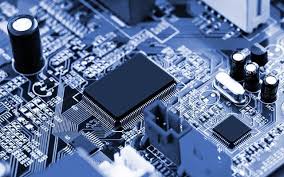
What is a Printed Circuit Board?
The layout of the conductors is done with a program called CAD, which allows the designer to put the traces on the bare board and simulate how they will work. When the layout is finished, a positive image of it can be produced on photoplotted film. This is used by the board house to produce the actual board. The areas selectively exposed by the photo plotter are black, while unexposed areas are clear.
Conductors are usually made of copper, but a PCB can have other kinds of conducting material such as tin or tin-lead alloy. The insulating material is most often an epoxy-copper laminate, but there are exotic technologies such as FR-4 and others. The plated-through holes (vias) are usually made of copper, which is anodized to provide the necessary corrosion resistance.
There are several ways to create a printed circuit board, and each has its advantages and disadvantages. The point-to-point chassis construction method used in hi-fi and TV sets until the late 1960s was expensive, bulky and difficult to assemble. The circuit board invention reduced the cost of these systems by reducing the number of wires they required.
The most popular PCBs are single-sided and double-sided, but they can be multi-layer as well. A multi-layer board has additional internal layers of copper and insulating material that give it greater flexibility in how the circuit is arranged. Some of the inner layers are dedicated to providing a ground or power plane, which reduces electromagnetic interference (EMI) and improves signaling frequencies.
The last layer of a multi-layer board is the solder mask, which covers the conductive traces with a nonconductive material that gives it its characteristic green color. The other layers of a PCB can have silkscreen labeling, which could include numbers, letters or symbols that indicate the function of each connection point on the board. The silkscreen is applied after all the other layers are fabricated and etched. The copper is then plated with gold, silver or other material to give it the best possible contact with its corresponding pads.


)